IP Core Generation Workflow for Standalone FPGA Devices
You can generate a reusable HDL IP core for any supported Xilinx® or Altera® FPGA device. The workflow produces an IP core report that displays the target interface configuration and the coder settings that you specify. See Custom IP Core Generation.
You can optionally build your own custom reference designs and integrate the generated
IP core into the reference design. The workflow does not require the Embedded Coder® software, because you need not generate the embedded code that is run on
the processor. This means that the workflow has a Generate Software
Interface task, but you cannot generate a software interface model. If
you have HDL Verifier™ installed, on the Set Target Reference Design task,
set Insert JTAG MATLAB as AXI Master (HDL Verifier Required) to
on. You can then generate a software interface script in
the Generate Software Interface task to rapidly prototype and test
the HDL IP core functionality by using the MATLAB AXI Master. See Generate Software Interface to Probe and Rapidly Prototype the HDL IP Core.

The workflow for the FPGA boards has these features:
Set Target Reference Design task. Populates the reference design, its tool version, and the parameters that you specify.
Set Target Interface task. Map your DUT ports to the interfaces on the target platform.
Set Target Frequency task. Specifies the Target Frequency (MHz) to modify the clock module in the reference design to produce a clock signal with that frequency.
Generate RTL Code and IP Core task. Generates a reusable and sharable IP core. The IP core packages the RTL code, a C header file, and the IP core definition files.
Create Project task. Creates a project for integrating the IP core into the predefined reference designs.
You can generate an IP core with an optional AXI4 or an AXI4-Lite interface.
Targeting FPGA Reference Designs with AXI4 Interface
This figure shows how HDL Coder™ generates an IP core with an AXI4 interface and integrates the IP core into the FPGA reference design. See Board and Reference Design Registration System.
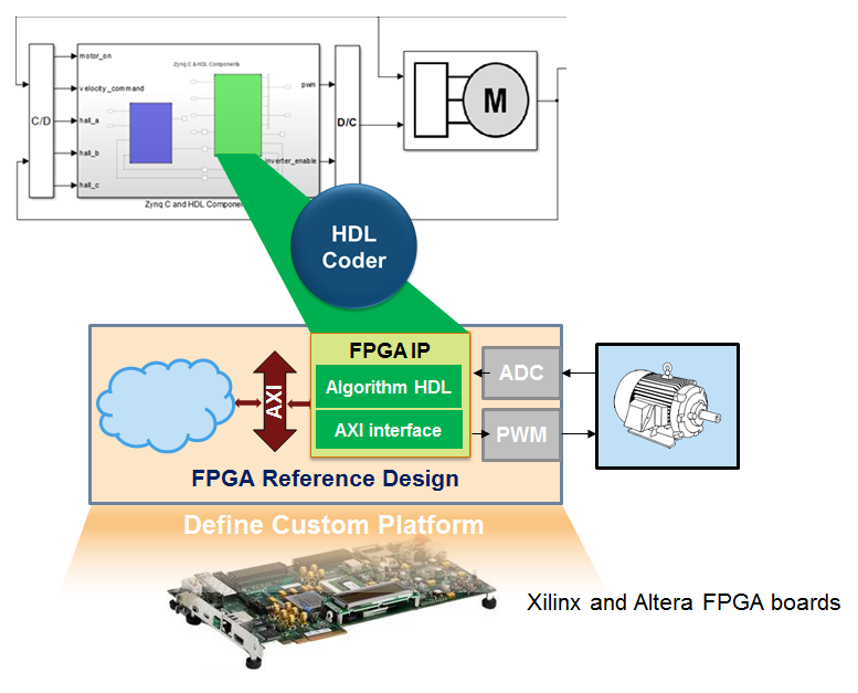
Use the HDL Coder generated AXI4-Lite interface to connect the IP core with an AXI4 or AXI4-Lite Master device such as:
MicroBlaze processor.
Nios II processor.
PCIe Endpoint that connects to an external processor.
JTAG Master.
When you connect the HDL IP core to a processor such as the MicroBlaze, you must integrate the handwritten C code to run on the processor. The generated IP core report displays the register address mapping information. To find the register offsets in the IP core register space, use this mapping information. To get the memory address of each register, add the register offset to the base address that you specify in your reference design. You can also find the register offsets in the C header file in the generated IP core folder.
Targeting FPGA Reference Designs Without AXI4 Interface
In the reference design definition function, you can create your own custom
reference designs without the AXI4 slave interface. See also addAXI4SlaveInterface.
When creating a custom reference design, to target a standalone FPGA board, use
the EmbeddedCoderSupportPackage method of the
hdlcoder.ReferenceDesign
class:
hRD.EmbeddedCoderSupportPackage = ...
                hdlcoder.EmbeddedCoderSupportPackage.None;
EmbeddedCoderSupportPackage.Board Support
HDL Coder supports these FPGA boards with the IP Core
Generation workflow:
Xilinx Kintex-7 KC705 development boardArrow DECA MAX 10 FPGA evaluation kit
Using these boards, you can integrate the generated IP core into the
default system reference design. By default, this
reference design does not have an AXI4 slave interface. Optionally, you can add the
interface in the reference design definition function.
Restrictions
IP Core Generation workflow does not support :
RAM Architecture set to
Generic RAM without clock enable.Using different clocks for the IP core and the AXI interface. The
IPCore_ClkandAXILite_ACLKmust be synchronous and connected to the same clock source. TheIPCore_RESETNandAXILite_ARESETNmust be connected to the same reset source. See Synchronization of Global Reset Signal to IP Core Clock Domain.