Streaming Data from Hardware to Software
This example presents a systematic approach to design the data-path between hardware logic (FPGA) and embedded processor using SoC Blockset. Applications are often partitioned between hardware logic and embedded processor on a system-on-chip (SoC) device to meet throughput, latency and processing requirements. You will design and simulate the entire application comprising of FPGA & processor algorithms, memory interface and task scheduling to meet the system requirements. You will then validate the design on hardware by generating code from the model and implementing on a SoC device.
Contents
Supported hardware platforms:
- Xilinx® Zynq® ZC706 evaluation kit
- Xilinx Zynq UltraScale™+ MPSoC ZCU102 Evaluation Kit
- ZedBoard™ Zynq-7000 Development Board
- Altera® Cyclone® V SoC development kit
- Altera Arria® 10 SoC development kit
Design Task and System Requirements
Consider an application that continuously process data on the FPGA and the embedded processor. In this example, the FPGA algorithm filters the input signal and streams the resulting data to the processor. In the implementation model soc_hwsw_stream_implementation, the Buffer block represents the transfer of data from FPGA to processor. The processor operates on the buffered data and classifies the data as either high or low frequency in the Processor Algorithm subsystem. FPGA generates a test data of either low or high frequency sinusoid based on the DIP switch setting in Test Data Source subsystem.

The application has following performance requirements:
- Throughput: 10e6 samples per second
- Maximum latency: 100ms
- Samples dropped: < 1 in 10000
Challenges in Designing Datapath
The FPGA processes data sample by sample while the processor operates on a frame of data at a time. The data is transferred asynchronously between FPGA and processor, and the duration of software task can vary for each execution. Therefore, a queue is needed to hold the data between FPGA and processor to prevent data loss. This queue is implemented in two stages, one as a FIFO of bursts of data samples in FPGA memory and other as a series of frame buffers in external memory. You will need to set three parameters related to the queue: frame size (number of samples in a frame of data), number of frame buffers and FIFO size (number of bursts of samples in FIFO).
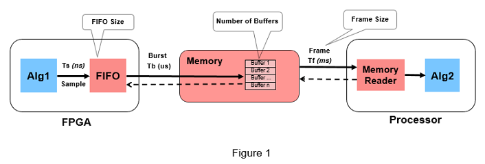
These design parameters affect performance and resource utilization. Increasing the frame size allows more time for software task execution and to meet throughput requirements at the cost of increasing latency. Typically, you set these parameters only when you are ready to implement on hardware, which presents the following challenges:
- It is difficult to debug issues like dropping of samples in hardware due to lack of visibility.
- It is difficult to design your application efficiently without first evaluating the effects of hardware interfaces. It can take many design-implementation iterations as you can assess performance only via implementation on hardware.
- It is difficult to optimize design since performance and cause-effect relationships are difficult to determine through implementation.
Ideally you want to account for these hardware effects while you are developing the application at design time, before implementing and running on hardware. One way to satisfy these requirements is to simulate the hardware effects, at design time. If you can simulate the variation in task durations, utilization of memory buffers/FIFOs and external memory transfer latencies, you can evaluate their effects on application design and implement the proven design on hardware. SoC Blockset allows you to simulate these effects so you can evaluate the performance of the deployed application before running on hardware.
Design Using SoC Blockset
Create an SoC model soc_hwsw_stream_top from the implementation model soc_hwsw_stream_implementation using the Stream from FPGA to Processor Template. The top model includes FPGA model soc_hwsw_stream_fpga and processor model soc_hwsw_stream_proc instantiated as model references. The top model also includes Memory Channel and Memory Controller blocks which model shared external memory between FPGA and processor. These were earlier modeled using buffer block in the implementation model. To improve simulation performance, FPGA algorithm is also modeled for Frame-based processing soc_hwsw_stream_fpga_frame and is included as model variant subsystem at the top level. You can select the model to run in Frame-based or Sample-based processing by selecting from the mask of FPGA subsystem.

Design to Meet Latency Requirement : Latency in the datapath from FPGA to processor comprises of the latency through the FPGA logic and the time for data transfer from FPGA to processor through memory channel. In this example, the FPGA clock is 10MHz and the latency is on the order of nanoseconds. This is negligible in comparison with latency within the memory channel, which is on the order of milliseconds. Therefore, let us focus on designing for latency for data transfer in the following manner.
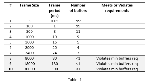
Begin with a few potential frame sizes and calculate Frame period for each frame size in Table -1. Frame period is the time between two consecutive frames from FPGA to processor. For this example, FPGA output sample time is 10e-6 as a valid data is output every 100 clock cycles from the FPGA.

Latency of the memory channel is due to time elapsed by samples in the queue of frame buffers and FPGA FIFO. Let us size FPGA FIFO equivalent to one frame buffer. To stay within the maximum latency requirement, calculate the number of frame buffers for each frame size as per:

Maximum latency allowed for this example is 100 ms. Since the number of buffers account for maximum latency requirement, for all the cases in Table -1, latency requirement is met. A minimum of 3 frame buffers is needed in external memory for data transfer. While one of the frame buffers is written by FPGA, the other frame buffer is read by processor. Therefore, Case #8-10 from the table below are rejected as they violate the minimum buffer requirement.
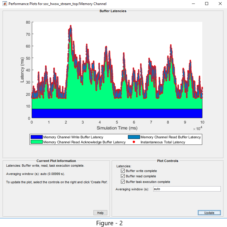
To visualize the latency, simulate the model and open Memory Channel block, go to Performance tab and click on View performance plots . Select all the latency options under Plot Controls and click Create Plot . As captured in Figure - 2, you will notice that the composite latency meets the < 100 ms requirement.
Design to Meet Throughput Requirement : On average, the software tasks processing must complete within a frame period, as otherwise, task will overrun leading to dropping of data and violate the throughput requirement. i.e.

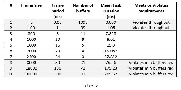
There are various ways of obtaining mean tasks durations corresponding to frame sizes for your algorithm, which are covered in Task Execution Example. Mean task durations for various frame sizes are captured in Table 2.
To simulate the model with the parameters corresponding to rows (#2-#7) in the table use the function set_hwsw_stream_set_parameters function with row # as an argument. Set the model parameters for row # 2 as below:
>> soc_hwsw_stream_set_parameters(2); % row # 2
Since the Mean Task Duration of 1.06 ms is less than Frame Period of 1.0 ms, the data is dropped in the memory channel. Open Logic Analyzer and notice that signal icFIFODroppedCount is increasing throughout the simulation as captured in Figure 3, indicating accumulating amount of dropped data.

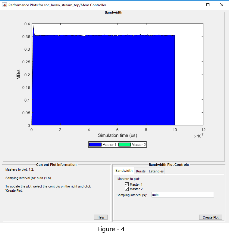
Since data is dropped during transfer from FPGA to processor through memory, this is reflected as a drop in throughput. Open Memory controller block, go to Performance tab and click on Plot data throughput button under Performance tab to see the memory throughput plot as in figure 4. Note that the throughput is less than the required 0.4 MBps. Since the FPGA output data sample time is 10e-6 and each sample is 4 bytes wide, the required streaming throughput for the system is 4 bytes/10e-6 = 400 KBps.
Design to Meet Drop Samples Requirement : Since the task durations can vary for many reasons like different code execution paths and variation in OS switching time, it is possible that data is dropped in the memory channel. Specify the mean task execution duration and statistical distribution for task durations in the mask of Task Manager block. Size the FIFO equivalent to one frame buffer. Set the FIFO burst size to 16 Bytes and calculate the FIFO depth:

Now, simulate the model for 100 sec (10e6 samples at 10e-6 samples per second) for cases # 3-7. Open the Logic analyzer and note the number of samples dropped on signal icFIFODroppedCount.
>> soc_hwsw_stream_set_parameters(3); % set the model parameters for #3
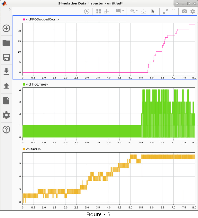
Open Simulation Data Inspector and add signals from memory channel as shown in Figure 5 below. Note that as buffers usage (signal buffAvail) increase to the maximum 11, the FIFO usage (signal isFIFOEntries ) begin to increase. When FIFO is completely used, the samples get dropped (signal isFIFODroppedCount )
The results of simulation for all the cases #3-7 and resultant sample dropped per 10000 are tabulated in Table 3.

The highlighted entries (rows #4 and #5) are valid design choices since they meet throughput, latency and drop samples requirement.
Implement and Run on Hardware
Following products are required for this section:
- HDL Coder™
- Embedded Coder®
- SoC Blockset Support Package for Xilinx Devices, or
- SoC Blockset Support Package for Intel Devices
To implement the model on a supported SoC board use the SoC Builder tool. Open the mask of 'FPGA' subsystem and select model variant to 'Sample based processing'. By default, the model will be implemented on Xilinx® Zynq® ZC706 evaluation kit as it is configured with that board. Open SoC Builder from the Tools menu and follow these steps:
- Select 'Build Model' on 'Setup' screen. Click 'Next'.
- Click 'View/Edit Memory Map' to view the memory map on 'Review Memory Map' screen. Click 'Next'.
- Specify project folder on 'Select Project Folder' screen. Click 'Next'.
- Select 'Build, load and run' on 'Select Build Action' screen. Click 'Next'.
- Click 'Validate' to check the compatibility of model for implementation on 'Validate Model' screen. Click 'Next'.
- Click 'Build' to begin building of the model on 'Build Model' screen. An external shell will open when FPGA synthesis begins. Click 'Next'.
- Click 'Test Connection' on 'Connect Hardware' screen to test the connectivity of host computer with SoC board. Click 'Next' to go to 'Run Application' screen.
The FPGA synthesis may take more than 30 minutes to complete. To save time, you may want to use the provided pre-generated bitstream by following these steps:
- Close the external shell to terminate synthesis.
- Copy pre-generated bitstream to your project folder by running the command below and then,
- Click 'Load and Run' button to load pre-generated bitstream and run the model on SoC board
>> copyfile(fullfile(matlabroot,'toolbox','soc','socexamples','bitstreams','soc_hwsw_stream_top-zc706.bit'), './soc_prj');
While the application is running on hardware, toggle the DIP switch on your board to change the test data from 'low' to 'high' frequency and notice the blinking of corresponding LED on the board. You can also read the samples dropped count in the model running on external mode. Thus, you verify that your implementation from SoC Blockset model matches the simulation and meets the requirements.
Implementation on other boards: To implement the model on a supported board other than Xilinx® Zynq® ZC706 evaluation kit board, you must first configure the model to the supported board and set the example parameters as below. Open Model Configuration Parameters, navigate to Hardware Implementation tab and perform the following settings:
- Select your board from the drop-down list under Hardware board on both top and processor model.
- Navigate to Target hardware resources > FPGA design (top level) tab and enable Include MATLAB as AXI Master IP for host-based interaction and set IP core clock frequency (MHz) to 10 MHz.
- Navigate to Target hardware resources > FPGA design (debug) tab and enable Include AXI Interconnect monitor.
Next, open SoC Builder and follow the steps as previously stated for Xilinx® Zynq® ZC706 above. Modify the copyfile command to match the bitstream corresponding to your board. Available pre-generated bitstreams are:
- 'soc_hwsw_stream_top-zc706.bit'
- 'soc_hwsw_stream_top-zedboard.bit'
- 'soc_hwsw_stream_top-zcu102.bit'
- 'soc_hwsw_stream_top-c5soc.sof'
- 'soc_hwsw_stream_top-a10soc.sof'
In summary, this example showed you a systematic approach to design the datapath between hardware logic and embedded processor using SoC Blockset. You chose design parameters of frame size, number of frame buffers and FIFO size to meet the system performance requirements of throughput, latency and drop samples. By simulating and visualizing the effects of these parameters on the complete model containing hardware logic, processor algorithms, external memory and processor task durations, you uncovered issues like loss of throughput, latency and dropping of samples before implementing on hardware. This workflow ensures that the design works on hardware before implementation and avoids long design-implementation iterations.