Code Generation from Multirate Models
HDL Coder™ supports HDL code generation for single-clock and multiple clock multirate models. Your model can include blocks running at multiple sample rates:
Within the device under test (DUT).
In the test bench driving the DUT. In this case, the DUT inherits multiple sample rates from its inputs or outputs.
In both the test bench and the DUT.
In general, generating HDL code for a multirate model does not differ greatly from generating HDL code for a single-rate model. However, there are a few requirements and restrictions on the configuration of the model and the use of specialized blocks (such as Rate Transitions) that apply to multirate models. For details, see Multirate Model Requirements for HDL Code Generation.
Clock Enable Generation for a Multirate DUT
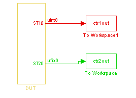
The following block diagram shows the interior of a subsystem
containing blocks that are explicitly configured with different sample
times. The upper and lower Counter Free-Running blocks have sample
times of 10 s and 20 s respectively. The counter output signals are
routed to output ports ST10 and ST20,
which inherit their sample times. The signal path terminating at ST10 runs
at the base rate of the model; the signal path terminating at ST20 is
a subrate signal, running at half the base rate of the model.

As shown in the next figure, the outputs of the multirate DUT drive To Workspace blocks in the test bench. These blocks inherit the sample times of the DUT outputs.
The following listing shows the VHDL® entity declaration generated for the DUT.
ENTITY DUT IS
  PORT( clk                               :   IN    std_logic;
        reset                             :   IN    std_logic;
        clk_enable                        :   IN    std_logic;
        ce_out_0                          :   OUT   std_logic;
        ce_out_1                          :   OUT   std_logic;
        ST10                              :   OUT   std_logic_vector(7 DOWNTO 0);  -- uint8
        ST20                              :   OUT   std_logic_vector(5 DOWNTO 0)  -- ufix6
        );
END DUT;
The entity has the standard clock, reset, and clock enable inputs
and data outputs for the ST10 and ST20 signals.
In addition, the entity has two clock enable outputs (ce_out_0 and ce_out_1).
These clock enable outputs replicate internal clock enable signals
maintained by the timing controller entity.
The following figure, showing a portion of a
Mentor Graphics®
ModelSim® simulation
of the generated VHDL code, lets you observe the timing relationship
of the base rate clock (clk), the clock enables,
and the computed outputs of the model.
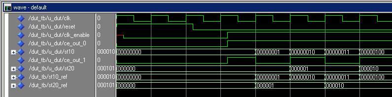
After the assertion of clk_enable (replicated
by ce_out_0), a new value is computed and output
to ST10 for every cycle of the base rate clock.
A new value is computed and output for subrate signal ST20 for
every other cycle of the base rate clock. An internal signal, enb_1_2_1 (replicated
by ce_out_1) governs the timing of this computation.