Create Xilinx KC705 Evaluation Board Definition File
Overview
For FPGA-in-the-loop, you can use your own qualified FPGA board, even if it is not in the pre-registered FPGA board list supplied by MathWorks®. Using the New FPGA Board wizard, you can create a board definition file that describes your custom FPGA board.
In this example, you can follow the workflow of creating a board definition file for the Xilinx® KC705 evaluation board to use with FIL simulation.
What You Need to Know Before Starting
Check the board specification so that you have the following information ready:
FPGA interface to the Ethernet PHY chip
Clock pins names and numbers
Reset pins names and numbers
In this example, the required information is supplied to you. In general, you can find this type of information in the board specification file. This example uses the KC705 Evaluation Board for the Kintex-7 FPGA User Guide, published by Xilinx.
For validation, you must have Xilinx or Altera® on your path. Use the
hdlsetuptoolpathfunction to configure the tool for use with MATLAB®.To verify programming the FPGA board after you add its definition file, attach the custom board to your computer. However, having the board connected is not necessary for creating the board definition file.
Start New FPGA Board Wizard
Start the FPGA Board Manager by entering the following command at the MATLAB prompt:
>>fpgaBoardManager
Click Create Custom Board to open the New FPGA Board wizard.

Provide Basic Board Information
In the Basic Information pane, enter the following information:
Board Name: Enter "My Xilinx KC705 Board"
Vendor: Select
XilinxFamily: Select
Kintex7Device: Select
xc7k325tPackage: Select
ffg900Speed: Select
-2JTAG Chain Position: Select
1

The information you just entered can be found in the KC705 Evaluation Board for the Kintex-7 FPGA User Guide.
Click Next.
Specify FPGA Interface Information
In the Interfaces pane, perform the following tasks.
Select FIL Interface. This option is required for using your board with FPGA-in-the-loop.
Select GMII in the PHY Interface Type. This option indicates that the onboard FPGA is connected to the Ethernet PHY chip via a GMII interface.
Leave the User-defined I/O option in the FPGA Turnkey Interface section cleared. FPGA Turnkey workflow is not the focus of this example.
Clock Frequency: Enter 200. This Xilinx KC705 board has multiple clock sources. The 200 MHz clock is one of the recommended clock frequencies for use with Ethernet interface (50, 100, 125, and 200 MHz).
Clock Type: Select
Differential.Clock_P Pin Number: Enter AD12.
Clock_N Pin Number: Enter AD11.
Clock IO Standard — Leave blank.
Reset Pin Number: Enter AB7. This value supplies a global reset to the FPGA.
Active Level: Select
Active-High.Reset IO Standard — Leave blank.
You can obtain all necessary information from the board design specification.

Click Next.
Enter FPGA Pin Numbers
In the FILI/O pane, enter the numbers for each FPGA pin. This information is required.
Pin numbers for RXD and TXD signals are entered from the least significant digit (LSD) to the most significant digit (MSB), separated by a comma.
For signal name... Enter FPGA pin number... ETH_COL W19 ETH_CRS R30 ETH_GTXCLK K30 ETH_MDC R23 ETH_MDIO J21 ETH_RESET_n L20 ETH_RXCLK U27 ETH_RXD U30,U25,T25,U28,R19,T27,T26,T28 ETH_RXDV R28 ETH_RXER V26 ETH_TXD N27,N25,M29,L28,J26,K26,L30,J28 ETH_TXEN M27 ETH_TXER N29 Click Advanced Options to expand the section.
Check the Generate MDIO module to override PHY settings option.
This option is selected for the following reasons:
There are jumpers on the Xilinx KC705 board that configure the Ethernet PHY device to MII, GMII, RGMII, or SGMII mode. Since this example uses the GMII interfaces, the FPGA board does not work if the PHY devices are set to the wrong mode. When the Generate MDIO module to override PHY settings option is selected, the FPGA uses the Management Data Input/Output (MDIO) bus to override the jumper settings and configure the PHY chip to the correct GMII mode.
This option currently only applies to Marvell Alaska PHY device 88E1111 and this KC705 board is using the Marvel device.
PHY address (0 – 31): Enter 7.

Click Next.
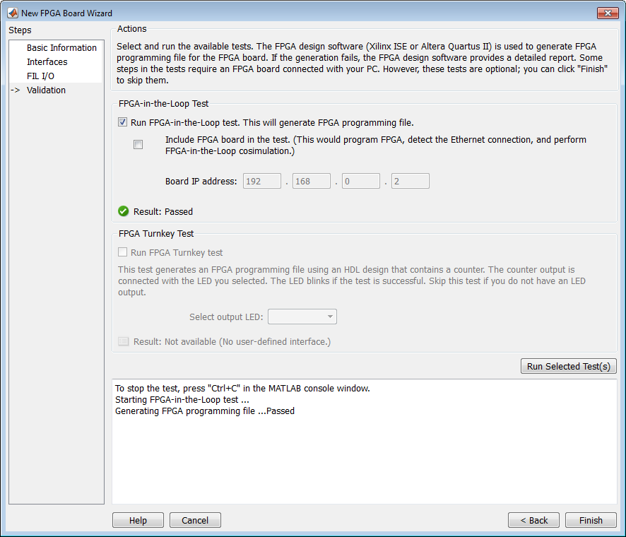
Run Optional Validation Tests
This step provides a validation test for you to verify if the entered information is correct by performing FPGA-in-the-loop cosimulation. You need Xilinx ISE 13.4 or higher versions installed on the same computer. This step is optional and you can skip it, if you prefer.
Note
For validation, you must have Xilinx or Altera on your path. Use the hdlsetuptoolpath function to configure the tool
for use with MATLAB.
To run this test, perform the following actions.
Check the Run FPGA-in-the-Loop test option.
If you have the board attached, check the Include FPGA board in the test option. You need to supply the IP address of the FPGA Board. This example assumes that the Xilinx KC705 board is attached to your host computer and it has an IP address of 192.168.0.2.
Click Run Selected Test(s). The tests take about 10 minutes to complete.
Save Board Definition File
Click Finish to exit the New FPGA Board wizard. A Save As dialog box pops up and asks for the location of the FPGA board definition file. For this example, save as
C:\boardfiles\KC705.xml.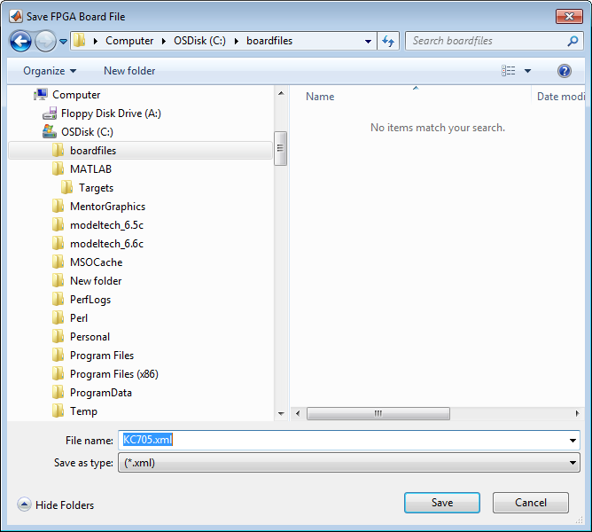
Click Save to save the file and exit.
Use New FPGA Board
After you save the board definition file, you are returned to the FPGA Board Manager. In the FPGA Board List, you can now see the new board you defined.

Click OK to close the FPGA Board Manager.
You can view the new board in the board list from either the FIL wizard or the HDL Workflow Advisor.
Start the FIL wizard from the MATLAB prompt.
>>filWizard
The Xilinx KC705 board appears in the board list and you can select it for FPGA-in-the-loop simulation.

Start HDL Workflow Advisor.
In step 1.1, select
FPGA-in-the-Loopand click Launch Board Manager.The Xilinx KC705 board appears in the board list and you can select it for FPGA-in-the-loop simulation.
